(China (Mainland))

Product Summary
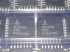
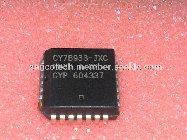
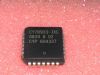
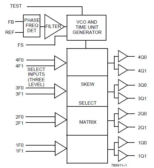
The CY7B933-JXC is a Programmable Skew Clock Buffer. It offers user-selectable control over system clock functions. This multiple-output clock driver provides the system integrator with functions necessary to optimize the timing of high-performance computer systems.
Parametrics
CY7B933-JXC absolute maximum ratings: (1)Storage Temperature: –65℃ to +150℃; (2)Ambient Temperature with Power Applied: –55℃ to +125℃; (3)Supply Voltage to Ground Potential: –0.5V to +7.0V; (4)DC Input Voltage: –0.5V to +7.0V; (5)Output Current into Outputs (LOW): 64 mA; (6)Static Discharge Voltage(per MIL-STD-883, Method 3015) : >2001V; (7)Latch-Up Current: >200 mA.
Features
CY7B933-JXC features: (1)All output pair skew <100 ps typical (250 max.); (2)3.75- to 100-MHz output operation; (3)Selectable skew to 18 ns; (4)Inverted and non-inverted; (5)Zero input to output delay; (6)50% duty-cycle outputs; (7)Outputs drive 50Ω terminated lines.
Diagrams
| Image | Part No | Mfg | Description |  |
Pricing (USD) |
Quantity | ||||||||||
|---|---|---|---|---|---|---|---|---|---|---|---|---|---|---|---|---|
 |
 CY7B933-JXC |
Cypress Semiconductor |
Telecom Line Management ICs HOTLink Receiver COM |
Data Sheet |
|
|
||||||||||
|
CY7B933-JXCT |
Cypress Semiconductor |
Telecom Line Management ICs HOTLink RECEIVER STANDARD SPEED |
Data Sheet |
|
|
||||||||||